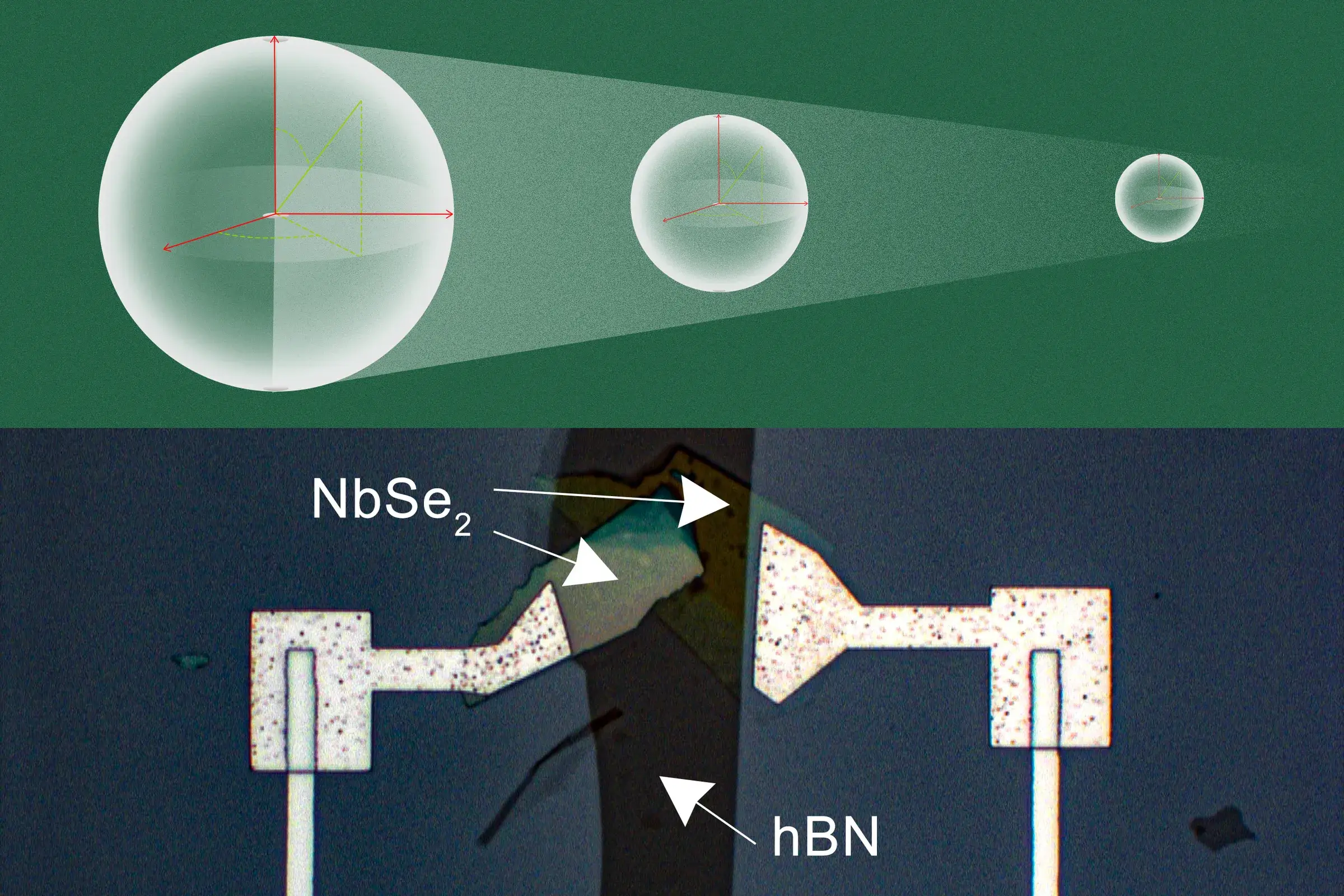
The Josephson junction inside a transmon is tiny. The circuit built around it is not. Much of the visible silicon belongs to the shunt capacitor, which has to be large enough to suppress charge sensitivity without throwing the stored microwave energy into a lossy dielectric.
That is why the capacitor grows. The obvious compact geometry — two nearby metal plates with an insulator between them — can be disastrous at millikelvin temperatures if the dielectric absorbs microwave energy.1
Many superconducting qubits therefore spread their electrodes sideways across a clean substrate. The field then lives largely in high-purity silicon and vacuum. The geometry is wasteful in area but gentle on coherence.12
MIT researchers attacked that trade in 2022 with hexagonal boron nitride, hBN. Parallel plates built from the 2D stack reduced the characteristic qubit footprint by roughly two orders of magnitude and still produced transmons reaching 25 microseconds of coherence.1 Later work on silicon fins and interface losses shows why the result was not the end of the story: once the capacitor shrinks, the material boundaries start carrying more of the burden.34
Why it grows
A transmon joins a Josephson junction to a shunt capacitance. The junction supplies the nonlinearity needed to separate useful quantum energy levels; the capacitance suppresses charge sensitivity.
In a common coplanar layout, two broad metal pads sit beside one another. Their field occupies the high-purity substrate and the vacuum above the chip. That geometry keeps most of the electric energy away from amorphous insulating films, where microscopic defects can become loss channels.1
MIT's account gives the scale of the compromise. Ordinary integrated-circuit dielectrics such as silicon oxide or silicon nitride can have quality factors of only a few hundred to a thousand in the relevant microwave regime, while a useful qubit needs far lower loss.2 Coplanar capacitor plates can consequently grow to around 100 by 100 micrometres for the required capacitance.2
The curious result is a device dominated in area by the supposedly boring component, not the exotic junction everyone draws in the diagram.
Open fields also reach neighbours. That gives density a second cost: putting qubits closer together can strengthen couplings the circuit never asked for.1
Back to plates
The MIT design returns to the textbook capacitor: one plate above another, separated by a dielectric. The unusual part is the dielectric itself.
Hexagonal boron nitride is a layered van der Waals crystal. Very thin sheets can be isolated and stacked while retaining a clean crystalline structure. The team placed hBN between superconducting niobium diselenide, NbSe₂, electrodes and connected that stack to an aluminium circuit containing the Josephson junction.1
At low temperature and single-photon microwave power, resonator measurements put hBN's loss tangent in the mid-10⁻⁶ range or lower. Transmons using those capacitors reached coherence times up to 25 µs, consistent with the measured dielectric loss.1
Electrically, the stack then behaves like the old textbook object it resembles: plenty of capacitance without requiring two broad pads side by side.
The Nature Materials paper describes a roughly 100-fold reduction in qubit feature size compared with conventional all-aluminium coplanar transmons used for comparison.1 MIT's accompanying explanation puts the result in similar terms: the new qubit occupied about one hundredth of the area of the conventional design on the same chip.2
Keep it inside
MIT also reported that more than 90 percent of the electric field stayed inside the layered capacitor.2
A coplanar capacitor leaves more of its field around the pads, where neighbouring structures can pick it up. A compact field should therefore reduce the capacitor's contribution to capacitive crosstalk. It cannot remove every coupling path in a processor — control lines, readout resonators, couplers and package modes remain — but it shrinks one broad electromagnetic footprint.
The scaling question changes at that point. Area is no longer the only scarce resource; material perfection becomes one too.
Under argon
Manufacturing is where the elegant diagram becomes awkward. NbSe₂ oxidises within seconds in air, according to Joel Wang, so the stack had to be assembled inside an argon glove box.2
Researchers handled flakes under a microscope, picked them up with a sticky polymer, stacked the layers, moved the completed heterostructure onto the qubit circuit and then removed the polymer.2 It is a perfectly reasonable research process. It is nothing like a wafer-scale sequence that semiconductor manufacturing wants to repeat millions of times with tiny variation.
Wang identified the next manufacturing problem directly: grow hBN and 2D superconductors across wafers, then stack those films at wafer scale.2 Until then, a one-hundred-times-smaller capacitor is partly a trade between chip area and process complexity.
Silicon fins
Another team approached the same problem from a different direction in 2025. Instead of a 2D material stack, they etched narrow fins from single-crystal silicon and metallised them with aluminium to create vertical parallel-plate capacitors.3
The fins were less than 300 nm wide and about 3 µm tall. Transmons using them occupied approximately 0.01 mm², while the paper cites about 0.2 to 0.5 mm² for many planar designs optimised for high coherence. Qubit T1 exceeded 25 µs, and resonators using the fin capacitors reached low-power internal quality factors above 500,000.3
Those numbers are not a silicon-versus-hBN scoreboard; the fabrication flows and measurements differ too much. They do show the same engineering question resurfacing: how can a circuit pack substantial capacitance into little area without forcing too much electric energy into a lossy material or interface?
Interfaces answer
A late-2025 study adds a particularly useful warning. Researchers experimentally observed interface piezoelectricity at aluminium-silicon junctions even though bulk silicon itself is not piezoelectric.4
Their modelling shows that electromechanical conversion at such an interface can become a loss channel in superconducting devices. In simulations at 4.5 GHz, 125-fF coplanar and parallel-plate geometries produced very different estimated quality limits, with the parallel-plate version much more exposed in that model because more electric energy participated at the interface.4
It would be wrong to copy that result onto MIT's NbSe₂–hBN–NbSe₂ capacitor. The materials and interfaces are different. The broader design lesson survives the distinction: once engineers concentrate the electric field to save area, the microscopic quality of the boundaries matters more.
Miniaturisation has not removed the loss problem. It has moved it into a smaller, more specific place.
What scaling means
Superconducting qubits will not scale by repeatedly shrinking one transistor-like object. Their footprint belongs to a complete electromagnetic circuit: junction, capacitance, couplers, readout, control wiring and packaging all have to retain useful quantum behaviour as density rises.
The hBN experiment uses a radical material to rescue a very old circuit idea: a parallel-plate capacitor with a dielectric clean enough to survive single-photon microwave fields at millikelvin temperatures.
What disappears from the floorplan reappears in crystal growth, transfer, oxidation, interfaces and wafer-scale reproducibility.
So “100× smaller qubits” is best read narrowly. The whole quantum computer did not shrink by one hundred; one large piece of the transmon footprint turned out to be an engineering payment rather than a law of nature: the price of keeping the electric field away from bad materials.