In September 2023, Intel promised that glass would replace the organic material used to wire chips together. Three years on, no commercial product has shipped on it. The latest roadmap roundup came out in late August 2026, and its opening verdict is blunt: glass-core substrates are only entering qualification, and the first product keeps slipping.2
That word is the one to keep: qualification. Not production. Not a launch. Package qualification is the stage where you prove a substrate actually survives inside a finished product. It is the invisible bottleneck press releases skip, and it is exactly where this dossier has stalled.
Why glass
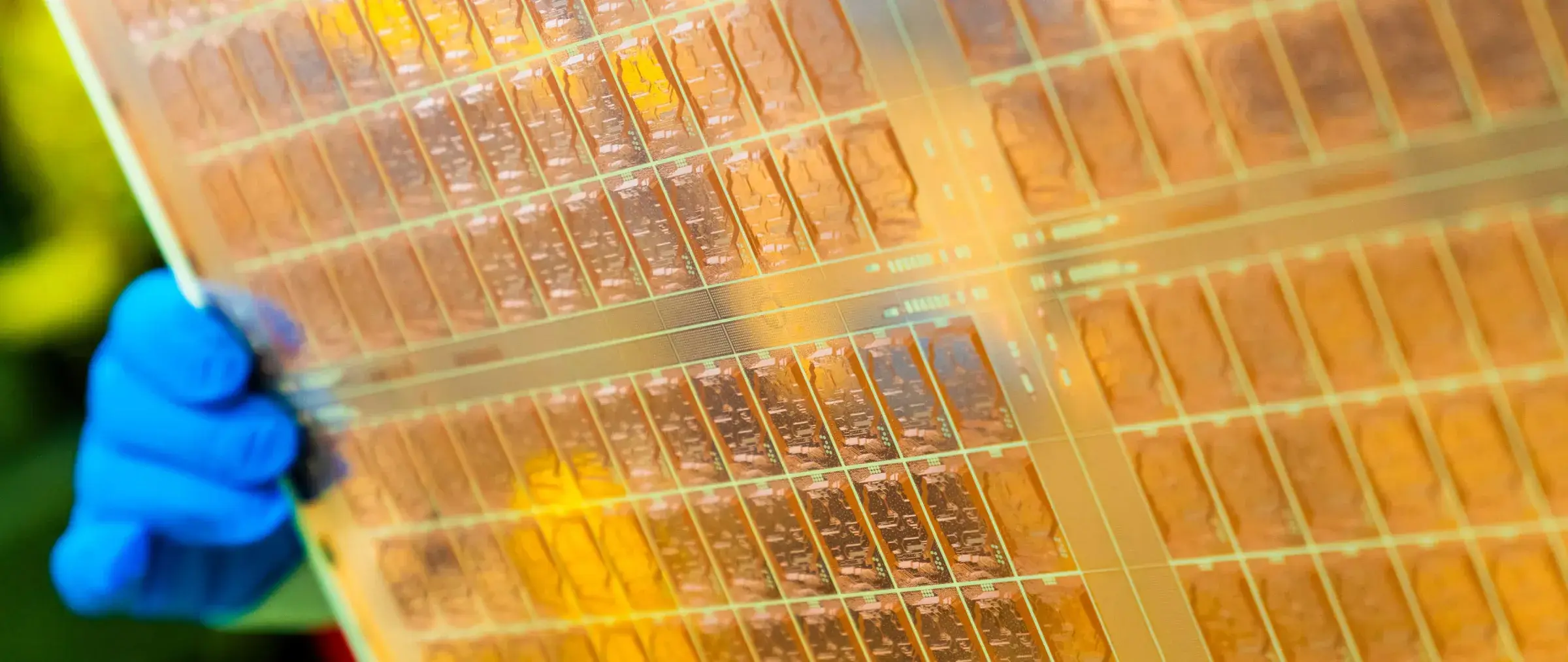
The substrate is the board chips sit on and get wired to. Today it is almost always organic, a composite that behaves like a circuit board. It has handled the job for decades, but it has one growing flaw: pile more silicon on it and it warps, losing the dimensional precision those connections need.2
Glass answers that with numbers Intel published back in 2023: up to ten times the interconnect density, 50% less pattern distortion, extreme flatness, and thermal behavior that can be tuned closer to silicon.12 A glass core can be matched to a coefficient of thermal expansion near silicon's, roughly halving the warpage an organic core would show.2
The pitch goes beyond swapping materials. On rectangular 510×515 mm panels, over 75% of the area is usable for large dies, versus roughly 50% on a round 300 mm wafer.2 That saves material and opens the door to bigger packages, at exactly the moment AI chips are outgrowing what organic can carry.
What Intel promised
Intel presented this in 2023 as work already well underway: a dedicated R&D line, more than a billion dollars behind it, dozens of inventions, and delivery to market planned for the "second half of this decade."12 All of it in service of Moore's Law and the goal of a trillion transistors inside a single package by 2030.
Intel had standing on this ground. It led the move from ceramic to organic packaging in the 1990s, then invented embedded-die stacking. Calling glass the next step was not groundless marketing.1
In 2025 Intel booted Windows on a glass-core substrate, and its module-engineering VP Rahul Manepalli called the benefits "undeniable," adding that Intel wants "to be one of the first ones who do it."2 The engineering moves. It is the commercial plan that has changed shape: Intel has pivoted toward licensing its patents and showing demo vehicles, with its own deployment now pointed at around 2030.2
In July 2026 Intel signed a memorandum with China's Lens Technology, the ultra-thin glass maker best known for smartphone covers, to work on through-glass vias (TGVs).6 That is an exploration-stage deal, not a production line.
The factory already exists
The furthest along on paper is not Intel but Absolics, a subsidiary of the South Korean chemicals group SKC. It built a $600 million plant in Covington, Georgia, backed by $75 million in CHIPS manufacturing funding and another $100 million for R&D.24
Its phase-one capacity, 12,000 m² of substrate a year, is enough for a few million H100-sized packages.2 Mass-production samples came off the line in the first quarter of 2026, and customer qualification reportedly includes AMD and AWS, according to industry press.2
But the mass-production date keeps sliding. Absolics once aimed for the second half of 2024, then 2025, then customer sign-off in early 2026. A July 2026 report now puts it at 2027, with final validation expected by year-end.28
The cost of that patience shows up in the parent company's books. SKC has posted 15 straight quarters of operating losses since late 2023, and has sold off much of its other businesses to focus on glass. Roughly half of the 1.17 trillion won raised this spring is earmarked for Absolics.7
The invisible bottleneck
To understand the delay, look at what separates prototype runs from mass production: package qualification.
A substrate, even a perfect one, is not a product. It has to be mated to real dies, given its redistribution layers and metallization, and proven stable through aging, heat, and mechanical stress. Press releases compress this into a line; in practice it takes months or years.
At Absolics it is in progress and not finished. On July 27, 2026, SKC said embedded glass samples made in Covington had been sent to Taiwan for an initial package-level reliability evaluation, with results possible before year-end.3 Before that, the company passed substrate-level internal tests and a first electrical check in Japan, and reached "good die" samples that meet design specs.3
That is real progress, and it is exactly what "in qualification" means: the material has cleared the steps that depend on it alone, and is now up against the one that depends on a finished product and its customer.
Glass is hard to handle
The material works against itself as well. Glass chips and cracks at the edges during drilling and dicing. A March MIT Technology Review report described early Absolics runs breaking hundreds of panels every couple of days.2
Fixes exist: an edge coating has cut measured edge stress from 95 to 49 MPa, and low-temperature dielectrics that cure below 180°C were developed to limit build-up stress.2 Yet metallizing vias below 10 microns and holding nanometer-scale flatness across half-meter panels remain open problems.2
It is not all struggle: through-glass vias of 6 microns with aspect ratios past 15 were demonstrated at ECTC 2025, and Georgia Tech has stacked glass running at 220 GHz with 0.3 dB of loss.2 The material does what it promises in the lab. Scaling it to industry does not.
A race that keeps slipping
Glass has become a global race, and everyone has a date. Samsung Electro-Mechanics moved its glass program to a dedicated business unit in February 2026 and signed a July joint venture, GlaSSEM, with Korea's Dongwoo Fine-Chem, a Sumitomo subsidiary, to make the glass core. 482 billion won, about $310 million, 66% Samsung-owned, with operations targeted for the second half of 2027.5
TSMC, the biggest packager outside Intel, is building its CoPoS line in Chiayi around rectangular 310×310 mm panels, going panel-level first, with pilot production in 2027 and mass production in the second half of 2028. Glass itself remains "under review" there, and TrendForce puts TSMC's commercial glass after 2030.2
In Japan, Dai Nippon Printing started its glass pilot line in December 2025, Toppan is commissioning one, and China's BOE is sampling from a pilot line.2
The pattern repeats: bold dates, then slips. Korea's commercial news outlet rates Samsung's glass maturity at 40 out of 100, an admitted gap between marketing dates and process readiness.2
No production design
The most honest figure may be this one: right now no production design exists on glass, and every named customer, AMD, Broadcom, AWS, Nvidia, comes from industry reporting, with nothing confirmed officially.2
This is not a material that failed. It is a recurring lesson about making things, familiar across so many IRZ stories: a prototype that proves a direction is possible does not prove it is reliable, affordable, or industrializable. Between a 220 GHz demonstration and the first million identical, defect-free parts lies a world of small surgery on edges, vias, and flatness.
The first glass product could come out of one of the Korean programs, or not until 2028, per SEMI, which projects initial production around then followed by 67% annual growth.2 The question worth watching over the next few months is simple: which of Absolics, Samsung, or TSMC will turn a lab-validated material promise into something that sits inside a machine people actually buy.
The roadmap may not have lied. It just underlined what a technology watch prefers to forget: between the announcement and the product sits a few months of qualification that decides everything.