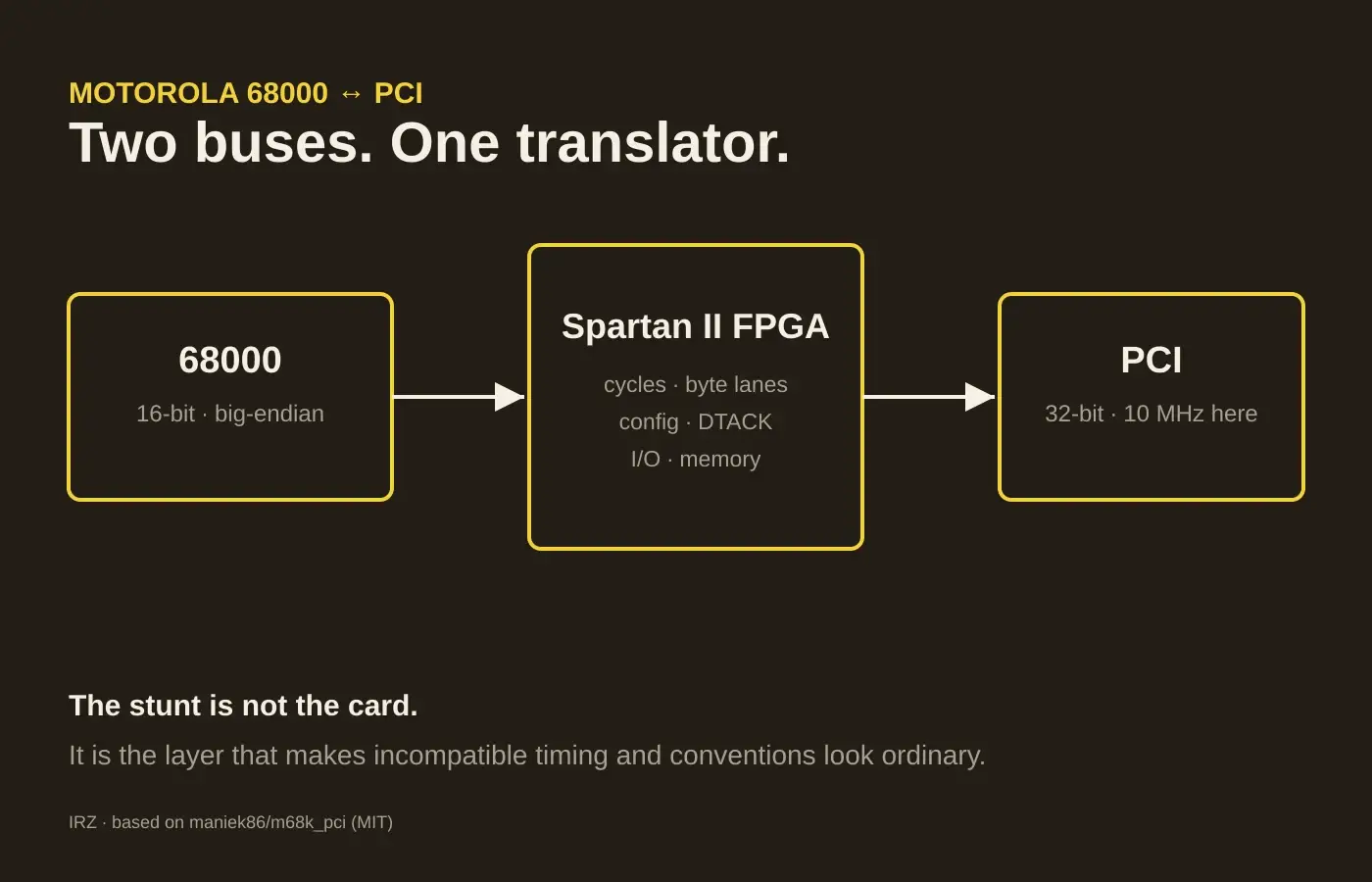
A 10 MHz Motorola 68000, two PCI slots pulled from old motherboards and a 1990s graphics card look like the ingredients of a bench-top joke, except maniek86's machine becomes interesting precisely because almost nothing about those parts is naturally compatible.1
The 68000 exposes a 16-bit, big-endian processor bus designed in the late 1970s, whereas PCI is a 32-bit, little-endian local bus with configuration space, synchronous transactions and a handshake protocol; the Xilinx Spartan II XC2S100 between them therefore does more than electrical conversion, because it has to translate the rules of one bus into the other.13
Two worlds
The finished system combines a 10 MHz 68000, 1 MB of SRAM, 128 KB of ROM, an MC68681 for serial I/O, an XC95144XL CPLD for system glue and two 32-bit 5 V PCI slots. The Spartan II acts as the host bridge.1
The clock choice says a lot about the build: conventional PCI runs at up to 33 MHz, yet this bus is held at 10 MHz to match the processor, a legal slowdown that gives up throughput in exchange for FPGA logic that is easier to reason about.1
That tradeoff defines the build, which is neither an attempt to produce the fastest 68000 nor a peculiar PC clone; the design deliberately slows the problem down until every layer can be inspected.
The bridge
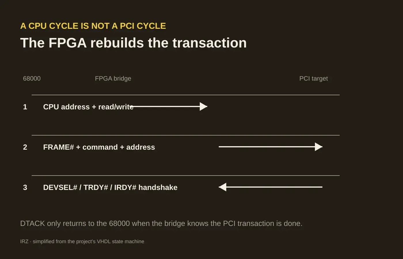
On a simpler peripheral bus, a processor presents an address, indicates read or write and waits for a response, while PCI adds a grammar in which the initiator first puts an address and command on multiplexed lines, asserts FRAME#, then negotiates the transfer through IRDY#, TRDY# and DEVSEL#.1
The Spartan II VHDL contains that state machine in literal form: configuration reads and writes, memory reads and writes, I/O accesses, the turnaround required on reads, device detection and acknowledgement back to the 68000.3 The processor's DTACK therefore no longer comes from a peripheral hanging directly from its bus; the bridge generates it only after the PCI-side transaction has finished.
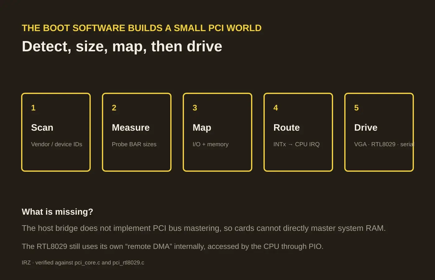
The same layer lets 68000 software discover cards much like PC firmware would. The code reads vendor, device and class identifiers, probes BARs by writing all ones to learn the requested size, then assigns I/O, memory and interrupt resources.4
Reversed bytes
Endianness is less photogenic but exposes the translation cost with unusual clarity: because the 68000 stores the most significant byte at the lowest address and PCI follows the opposite convention, a value such as 0xAABBCCDD occupies the four offsets in a different order on each side.1
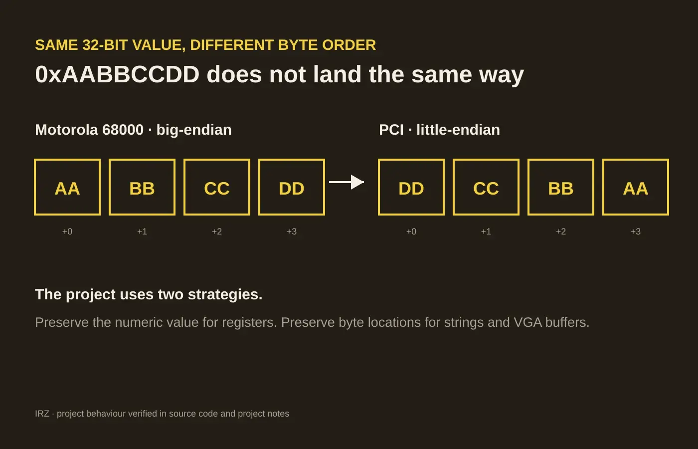
Maniek86 uses both translation strategies: a 32-bit hardware register benefits from preserving its value, while a VGA buffer or byte string is easier to handle when byte locations survive unchanged; the PCI code even reverses the offset explicitly for 8-bit configuration-space accesses.4
VGA makes the bug visible because a conventional text-mode macro packs a character and its attribute into one 16-bit word; on this machine that first produced colourful nonsense, until the packing order was reversed for the little-endian graphics card.1
Not a PC
Rather than recreate an entire x86 chipset, the bridge exposes the pieces this machine needs: one window of the 68000 address space becomes PCI I/O space, while an optional mapping reaches the legacy VGA memory region below 1 MB.13
That mapping also sidesteps a larger compatibility problem, since PCI graphics cards normally rely on an onboard video BIOS containing x86 instructions that the 68000 cannot execute without an emulator. With a Cirrus Logic GD5440, maniek86 programs the device registers directly and then performs standard VGA setup, reaching genuine 80×25 text mode and later 320×200, 256-colour graphics without running x86 firmware.1
The project estimates that filling the 64 KB mode-13h framebuffer takes roughly 300 ms, around 200 KB/s. The author explicitly labels that as a video-derived estimate rather than an instrumented benchmark.1 It is slow, but speed was never the point of a machine built to expose the path each byte takes.
Real cards
The hardware progresses far beyond merely listing devices in configuration space: a Moschip/NetMos PCI serial card runs with hardware interrupts, the GD5440 displays output, and two other graphics cards, including an S3 Trio64V2/DX, were also brought up.1
Networking provides the strangest proof: an RTL8029, essentially an NE2000-compatible controller on PCI, gets a driver, a tiny network stack, a Telnet server and a simple HTTP server, leaving a processor introduced in 1979 answering network traffic through an expansion standard that arrived more than a decade later.15
The choice of NIC is crucial, however, because many later PCI cards remain unusable on this host.
Missing mastering
The Spartan II does not implement PCI bus mastering. A card cannot request ownership of the bus and move blocks directly into system RAM. The creator cites the FPGA's exhausted pin budget as a major reason for leaving that part out.1
That omission rules out many sound cards, USB controllers, SCSI adapters, faster network cards and accelerators whose normal operation assumes DMA into host memory; the bridge deliberately implements only the PCI capabilities needed for this experiment.1
The word DMA still needs care here: the RTL8029 driver contains “Remote DMA” operations because the NE2000 architecture uses that mechanism between its registers and onboard memory, but those words still pass through programmed I/O under CPU control, so the NIC never becomes a PCI master of system RAM.5
The missing-mastering story even produced a useful hardware failure when an unconnected GNT# line floated: some cards behaved as though the bus had been granted to them, the bench supply tripped on over-current, and a pull-up finally restored sane behaviour.1 Few bugs illustrate the gap between “the connector fits” and “arbitration works” quite so neatly.
Active preservation
The result matters beyond decorative retrocomputing because PCI was designed to separate peripherals from the details of a particular processor bus, and that separation proves strong enough for a hobbyist FPGA bridge to connect generations that were never meant to meet; what normally disappears inside a chipset becomes visible again as configuration, transactions, mappings, interrupts and byte conventions rebuilt by hand.
The MIT-licensed repository includes the bridge VHDL, CPLD logic, bootloader and drivers, so the translation can be followed down to the lines deciding where individual bytes land instead of ending with a photograph of a successful “Hello World”.2
The useful lesson sits in that translation layer: preserving an old processor does not require freezing its original ecosystem around it. Its execution model can stay intact while a new layer lets it speak to later hardware, and on this board that mediator is literally the most modern part of the computer.