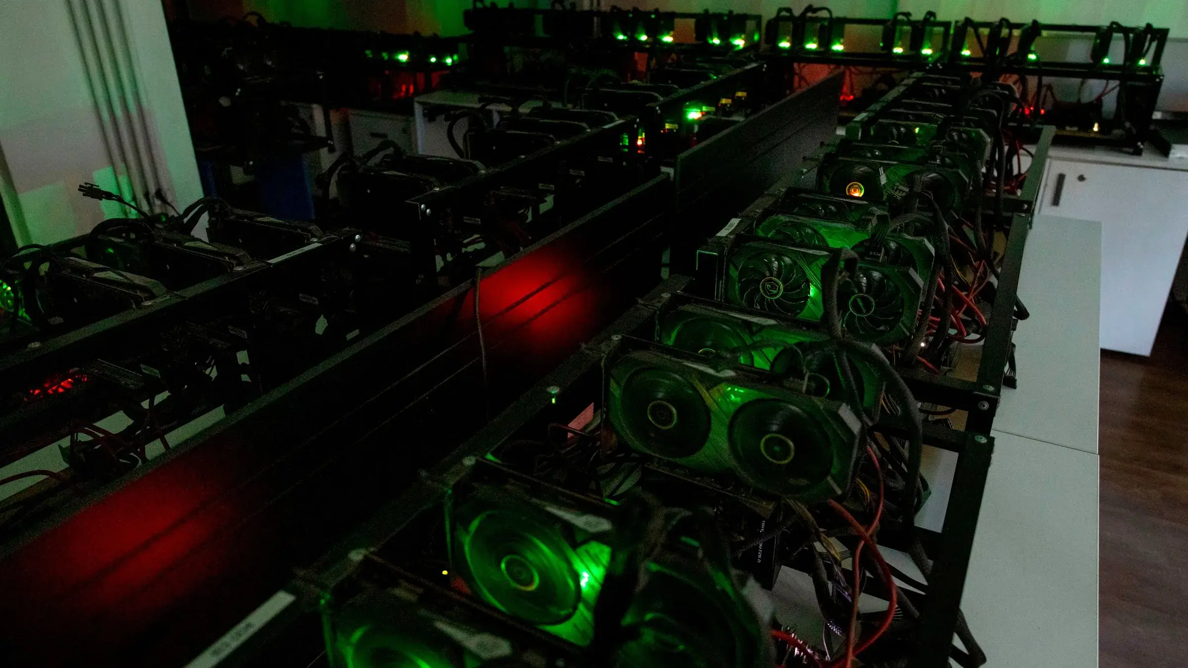
In 2021, Nvidia sold the CMP 170HX as an Ethereum-only mining card: no video outputs, no general-purpose drivers, 8GB of memory on the spec sheet. Five years later, the community has shown the spec sheet was lying. The memory chips soldered on the board can carry up to 64GB, and the lock keeping them asleep lives in firmware, not silicon.1
The story matters well beyond bargain hunters: it shows what a vendor can hide inside a product, and what it takes to get it back out.
An A100 in disguise
Under its modest hood, the CMP 170HX carries a complete GA100 die, the same silicon as the A100 accelerator Nvidia sells for several thousand dollars. The community documentation at 170th Street describes a PCB very close to the A100's, with HBM2e rated at 1,493 GB/s of bandwidth, more than an RTX 4090.5
Nvidia hobbled the beast at two levels: SM compute throughput is capped by throttle registers, and the memory geometry is cut down to the sold capacity. All applied through OTP configuration and firmware, in other words software writes onto physically complete hardware.12
The key comes through the driver
The tool that breaks the lock is called cmpunlocker, released under the GPL.1 Its mechanism exploits a signature-loading flaw in the Falcon BootROM, the security microcontroller supervising the chip's startup.3
Concretely, the tool patches the open-source nvidia-open driver (610.43 branch) to open four protection registers just before the GSP firmware boots, then rewrite the memory geometry and the declared VRAM length. The GPU then starts normally, but sees itself assigned 64GB where it used to report 8.12
The result survives reboots, and requires Linux x86-64, root access and Secure Boot disabled, since the patched kernel modules are unsigned.1 No soldering, no added components: everything happens in software.
The stinging detail: the 10GB variant of the card unlocks to 40GB, not 80GB. An 80GB configuration was built, tested, then rejected as unstable. Each SKU keeps its own ceiling, as if the throttling followed a commercial table rather than the physics of the chips.2
A cut-price compute card
With the unlock, the card also recovers its full compute throughput, a full BAR1, and a PCIe link moved from Gen1 to Gen2 in software.1 That link stays stuck at four lanes: Nvidia left empty the 24 AC coupling capacitors needed for a wider link, and hand-soldering them remains delicate surgery.23
That bottleneck mostly limits model loading. On Nvidia's developer forum, one user loads a quantized 70B model in about forty seconds over the restricted PCIe port, versus roughly ten with the full hardware modification. In decoding, they measure 27.3 tokens per second on a Qwen2.5-72B, while drawing 150 to 180 watts.3
For single-card inference, the trade-off holds up. The same person does report the GPU requesting a reset around 95% memory occupancy on very large context windows. This object remains a salvage prototype, not a certified workstation.
Defect or segmentation?
One uncomfortable question remains. A vendor can throttle healthy hardware to segment its catalog, or bin out chips whose unlocked memory would misbehave. On Hacker News, user ValdikSS reports finding no card whose RAM is actually defective; the throttling looks like commercial segmentation. But nobody has run these 64GB long enough to settle it, and ECC, precisely the mechanism that would check, still sits on the project's unsolved list.23
The market has already voted anyway: the card traded around $250 before the exploit spread, and now goes for over $1,000.34
Beyond the windfall, the episode documents something more durable: the line between what hardware can do and what its firmware agrees to do has become a commercial variable. And that line, a well-equipped community now knows how to cross.