The irresistible number is 2,000 times smaller, a claim that sounds simple until one asks what, exactly, has become two thousand times smaller.
MIT researchers published the nanofabrication method in spring 2026, and the headline number is accurate only when its unit travels with it: implosion carving patterns a swollen hydrogel and later shrinks the scaffold to roughly 1/2,000 of its original volume.12 A two-millimetre feature therefore does not magically become one micrometre wide, because volume and length are different quantities; humanity invented three dimensions before it invented press releases, inconveniently.
An isotropic 2,000-fold volume reduction corresponds to about 12.6-fold shrinkage along each dimension, almost exactly the scale reported for the high-shrinkage hydrogel, which reaches a final linear factor of 13.18 ± 0.28 after dehydration.1
To be sure, a thirteen-fold linear reduction is already plenty for the resolution problem the group is trying to solve.
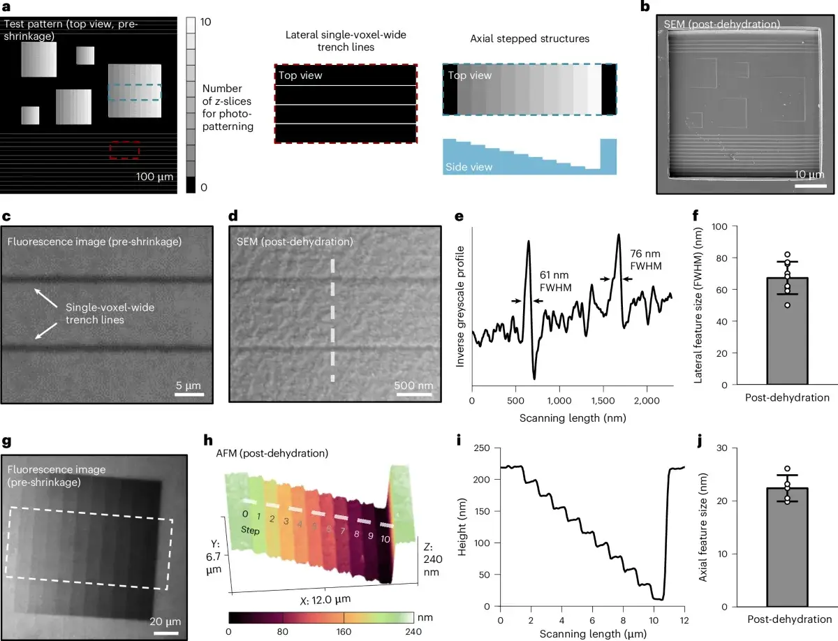
Instead of asking an optical system to write the final nanoscale structure directly, the team deliberately fabricates a larger version inside a soft scaffold and lets controlled material shrinkage perform the last precision step; features written while the laser is still operating at a comfortable scale end up below 100 nanometres, with resolution tests producing trenches 67 ± 12 nm wide and vertical steps only 22 ± 2 nm high.1
The clever part is turning a change of scale into a fabrication operation rather than pretending that the lab has built a mythical 2,000-fold photocopier.
The 2,000× trap
Take the headline number literally for a moment: a cube measuring 10 mm on each side has a volume of 1,000 mm³, and after each side is reduced by about 12.6 the new cube is roughly 0.79 mm wide with a volume close to 0.5 mm³. The volume has fallen two thousand times while the length has not.
The Nature Photonics paper uses two polyacrylate formulations, with the high-shrinkage scaffold reaching about 13× linearly and a moderate formulation roughly 5×.1 Applied isotropically, those factors correspond to about 2,290-fold and 127-fold reductions in volume respectively.
Correcting the unit makes the process easier to understand rather than less interesting, because the required gain is large enough to matter without assigning supernatural properties to wet polymer.
MIT News gives the intuitive example: photopatterning at roughly 800 nm can produce final features below 100 nm after shrinkage.2 The required gain along a line is around one order of magnitude, not three.
The useful question becomes why researchers cannot simply write at 67 nm in the first place, and the answer lies in the combination of three-dimensional internal structures, optical diffraction limits and fragile high-aspect-ratio geometries, all of which become increasingly awkward as the target shrinks.
By contrast, implosion carving moves part of that difficulty away from the writing tool and into a later material transformation.
Carve the gel
Over the last eight years, the more interesting change in Boyden’s approach has arguably been the carving, not merely the implosion.
Edward Boyden's lab introduced implosion fabrication in 2018 as a reversal of an idea from biological imaging: expansion microscopy embeds tissue in a hydrogel and physically enlarges it so microscopic structures can be resolved with ordinary microscopes, whereas Boyden and colleagues asked whether useful materials could be positioned in a swollen scaffold and then brought closer together by shrinking it.45
That earlier method optically patterned molecular anchors throughout a gel so functional materials such as nanoparticles, DNA or metals could later bind to selected positions before the scaffold contracted; the team went on to demonstrate conductive 3D silver nanostructures and features in the tens-of-nanometres range.5
The 2026 paper reverses that fabrication logic once more, this time by treating empty space as the thing worth patterning.
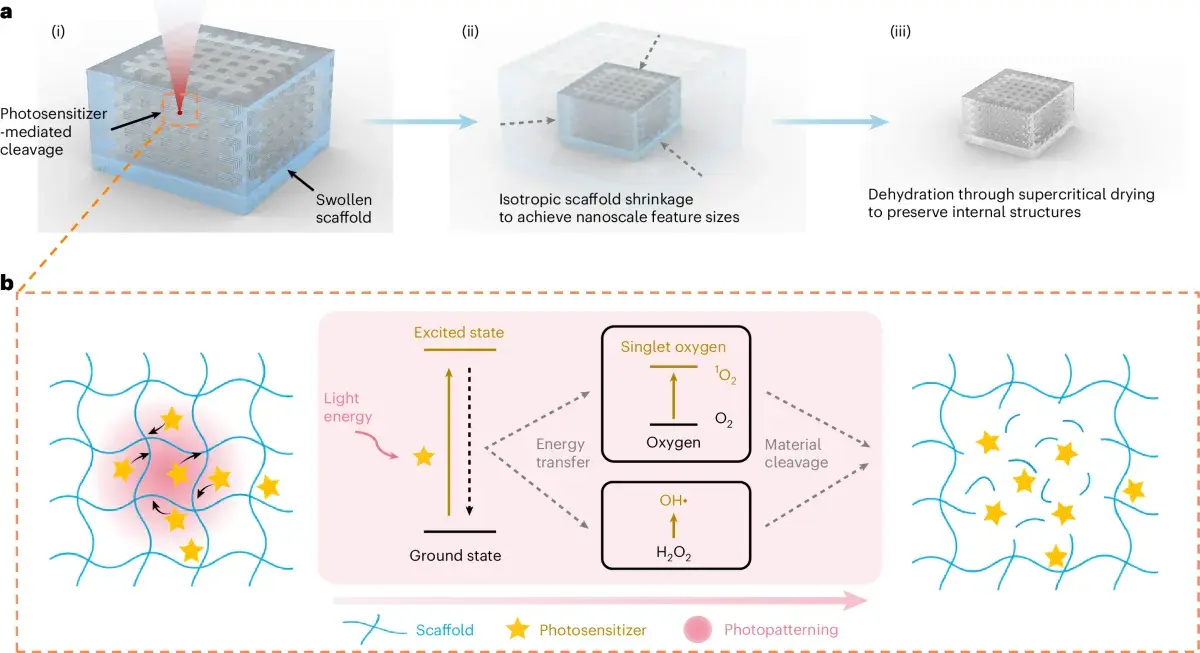
Rather than depositing the useful material where a structure should exist, implosion carving removes hydrogel where a vacancy should exist.1 Polymer and empty space then form a three-dimensional refractive-index landscape. For photonics, an accurately positioned hole can do useful work without being filled with some exotic deposited material.
The swollen gel is immersed in a solution containing rhodamine B as a photosensitizer, and multiphoton laser exposure excites the molecule only at selected positions; the excited sensitizer then generates reactive oxygen species that cleave polymer chains around the targeted point.1
Those reactive species travel only about 100 nm in the aqueous environment, helping keep the chemical damage localized.1 Once laser power is above the cleavage threshold, the targeted region becomes a genuine vacancy rather than a mildly modified patch of polymer.
The machine is drawing absence inside an object that is still enormous compared with the final device.
Thirteen times
After the vacancies have been patterned, the scaffold has to shrink without turning carefully designed 3D geometry into experimental dried fruit.
Divalent ions first contract the polyacrylate, producing close to an order-of-magnitude linear reduction in the high-shrinkage formulation.1 The gel then undergoes supercritical drying, which removes liquid without allowing ordinary surface tension during evaporation to collapse the tiny internal structures.
At the end of that sequence, the high-shrinkage formulation reaches 13.18× in linear dimension while the moderate gel, later used for the optical classifier, reaches 5.03×.1
Two formulations are useful because maximum shrinkage is not automatically the correct shrinkage for every device: the final geometry still has to retain controlled depths, sharp interfaces and enough remaining material for its optical function, which is why the researchers chose the moderate scaffold for the classifier whose nanoscale “neurons” required cleaner dimensions and edges.1
In manufacturing, the largest transformation factor is rarely the whole specification, which is a useful check on the seductive bigger-number instinct.
Shrinkage also needs to remain sufficiently isotropic, because if one axis contracted differently from another a designed helix would become a different helix and a phase mask would stop matching its numerical model; final accuracy therefore depends on the collective behaviour of the scaffold as much as on the spot size of the laser.
67 nanometres
The strongest evidence in the paper comes from an unglamorous set of lines and steps rather than the butterfly wing or optical classifier, which is reassuring because metrology has never needed a marketing department.
Researchers pattern single-optical-voxel trenches in the swollen gel and inspect them by electron microscopy after full shrinkage. Two example lines measure 61 nm and 76 nm full width at half maximum; across seven lines from three gels, the mean is 67 ± 12 nm.1
For vertical resolution, they create eleven steps using ten planes initially separated by 250 nm; after shrinking and dehydration, the average difference between neighbouring steps is 22 ± 2 nm.1
Those numbers justify “nanoprecise” more convincingly than the 2,000-fold volume figure.
The initial laser never draws a 22 nm step directly; it writes a larger geometry and a physical transformation later compresses spacing and error along with the rest of the structure.
The broader fabrication principle appears in many guises: rather than demanding every bit of final resolution from the first tool, make a structure at an easier scale and exploit a predictable downstream transformation — shrinkage, deposition, etching, stretching or self-assembly — as part of the precision chain.
The boring condition, usually the first clause removed when a laboratory process becomes a 12-second social video, is that the downstream transformation actually has to be predictable.
The butterfly
Resolution solves only half the problem, because a nanoscale three-dimensional feature also has to survive while it is being made.
Direct multiphoton additive methods can build tiny objects, but a long thin helix or lamella with an extreme aspect ratio tends to become mechanically unpleasant when it must support itself during fabrication. Published helical microstructures often use a widening pedestal that gradually transitions into the narrow thread.1
Implosion carving starts from another mechanical situation: the desired structure remains surrounded by scaffold while researchers remove the space around it.
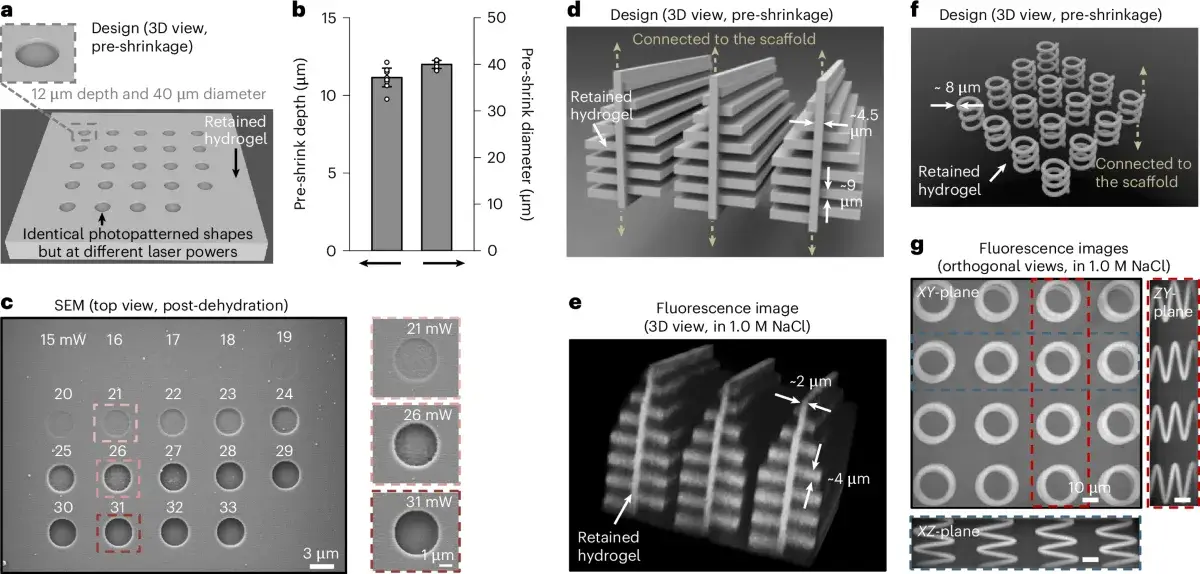
The team demonstrates a geometry inspired by Morpho butterfly-wing nanostructures, reaching an aspect ratio around 30 after a modest twofold shrink used for confocal imaging. It also creates a helical thread of roughly constant diameter, attached at its top and bottom, without the broad supporting pedestal required by some additive approaches.1
The difference is almost embarrassingly intuitive: additive printing builds an object in open space where the emerging structure has to stand, whereas carving leaves the object inside a larger body until its surrounding material is removed.
In the face of fragile high-aspect-ratio geometry, the temporary support is simply everything the process has not carved away yet.
That inversion from additive to subtractive thinking may be the most reusable part of the work, because a target geometry that is too fragile to construct directly can instead be surrounded by a temporary environment and revealed by removing everything that does not belong to the final object.
Mould makers, jewellers, ceramicists and MEMS engineers may contain their surprise at the philosophical discovery of temporary support; the new part is the scale and the ability to program arbitrary internal vacancies throughout a shrinkable volume.
Useful nothing
Manufacturing air becomes useful here because an optical structure cares about the boundary between refractive indices.
After supercritical drying, the remaining gel has a refractive index around 1.5 and the vacancies contain air, producing an index contrast around 0.5.1 The depth of a cavity controls how much phase shift light accumulates while crossing that region.
The volume can therefore be treated as a programmable refractive-index landscape: polymer here, air there, with different cavity depths where different optical phase delays are required. The paper demonstrates controlled depths and measures their phase effect at 532 nm, firmly in visible green light.1
At that point miniature sculpture becomes a photonic component, because the cavity depth has become a controllable optical variable.
Visible wavelengths are several hundred nanometres long, so controlling phase and diffraction with precision benefits from structural features substantially below that scale.23 The authors are not merely claiming a new way to make tiny ornaments; they show enough 3D refractive-index control to implement a designed visible-light transformation.
Not an AI chip
The next result is the one most likely to mutate into “MIT built an AI computer that thinks at the speed of light”, and after one unit error caution seems affordable.
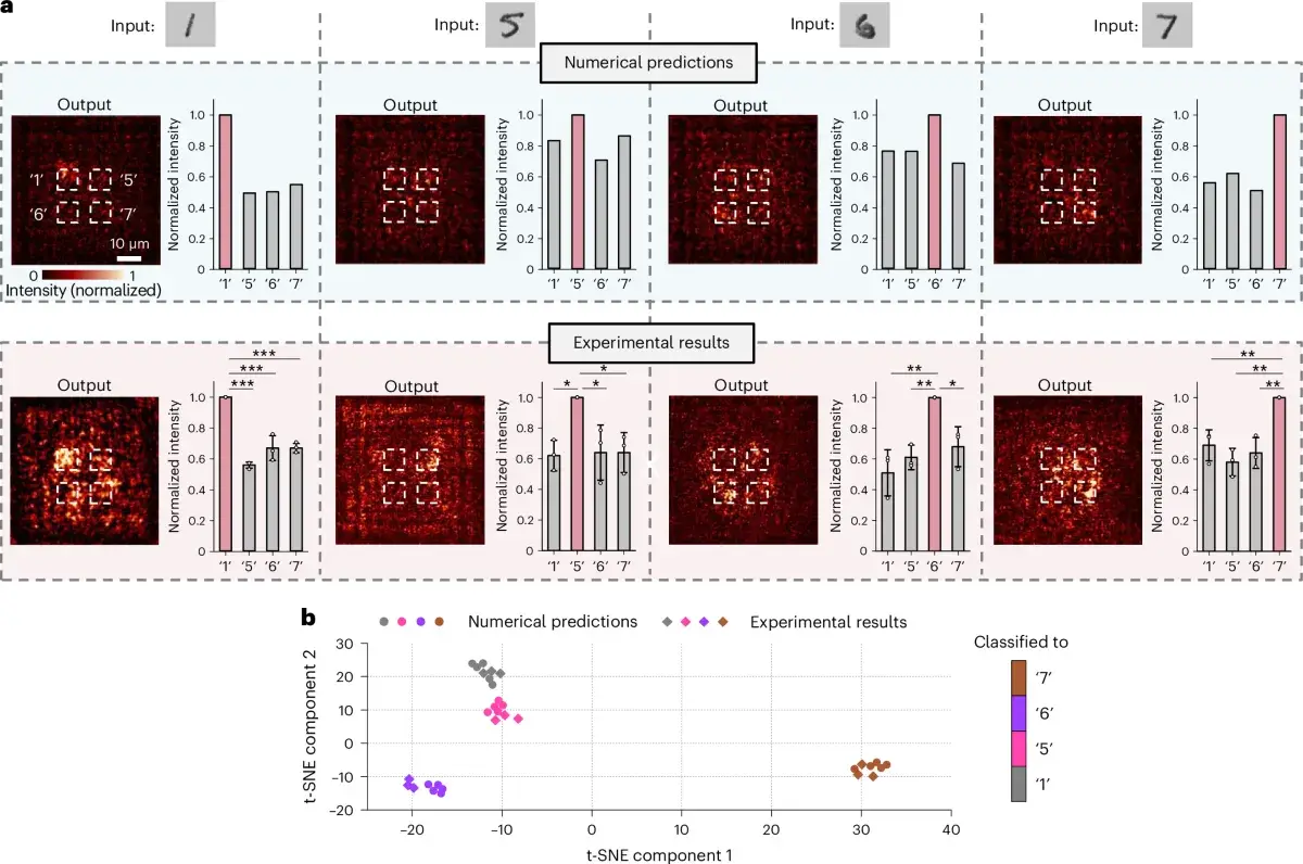
The paper fabricates a passive, pre-designed diffractive optical network for one narrow task: distinguishing four handwritten digits, 1, 5, 6 and 7, from MNIST.1 Nothing inside the final gel is training itself. Researchers optimize the geometry computationally before fabrication; once made, the fixed structure transforms incoming light through diffraction and phase delays.
The device contains two vacancy arrays inside one dehydrated scaffold, each with 120 × 120 optical “neurons” whose thickness determines phase shift; individual elements measure about 500 × 500 nm laterally and use eight discrete heights from 0 to roughly 700 nm, while the complete lateral device is around 60 × 60 µm with about 76 µm separating the arrays for 532 nm light.1
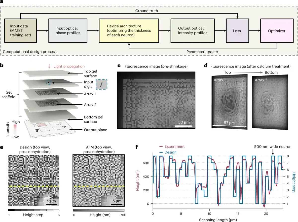
For a simpler proof of principle, the input digit is fabricated in the same gel as the network and a camera watches four output regions, one assigned to each digit; for every tested input, the device directs the strongest average light intensity into the intended region, significantly above the other three outputs.1
Experimental measurements use three devices from two gels per digit, and the paper also shows measured output vectors clustering near numerical predictions in a t-SNE projection.1
The agreement between the computer-designed phase landscape and its manufactured counterpart is useful evidence of fabrication fidelity, although the experiment remains far from an industrial recognition benchmark or a general-purpose optical accelerator ready to evict silicon from a data centre.
The manufacturing claim is already strong enough: the method can reproduce a calculated 3D nanoscale structure accurately enough for the object to perform the intended visible-light transformation.
Change the problem
Conventional nanofabrication explains why the detour is attractive, particularly when three-dimensional freedom and very small features are required at the same time.
Electron-beam lithography can define exceptionally fine surface features but naturally favours 2D and layerwise architectures. Multiphoton laser writing can move freely in three dimensions, yet arbitrary internal voids, extreme aspect ratios and tens-of-nanometres resolution remain difficult together.13
By contrast, implosion carving trades those constraints for another set rather than making them disappear.
It accepts a soft, swollen material and comparatively coarse optical patterning because the entire structure will later pass through a controlled isotropic transformation, while the surrounding scaffold supports delicate geometry as vacancies are written; the price is a chemistry-and-drying sequence whose proportions have to remain trustworthy all the way down.
Resolution stops being a property of one machine and becomes the product of several operations composed together.
That changes how the tooling problem is framed: when a machine reaches a precision limit, the obvious response is to build a more precise machine, whereas this work keeps conventional diffraction-limited optics and asks the material to change the scale of the result afterwards.
The researchers do not beat the limit head-on; they move the work into a coordinate system where that limit hurts less.
Where it hurts
A generic “nano” button for arbitrary solids has not appeared here, because the chemistry and the shrinkable scaffold are part of the method rather than incidental packaging.
The photosensitizer-mediated cleavage mechanism worked in several hydrogels tested by the team, including agarose, alginate and gelatin.1 Reaching final nanoprecision requires much more, however: a material must also shrink isotropically and survive supercritical drying while preserving the internal vacancies. The authors say those steps need individual optimization for each material system.1
Throughput is another straightforward limitation: current fabrication speed is constrained by a conventional point-scanning two-photon microscope that was never optimized as a production patterning tool, so the paper points to line-scanning or light-sheet approaches as possible routes to faster exposure.1
The optical demonstration also uses a dehydrated hydrogel around index 1.5 and air-filled voids, while more ambitious functions could require greater index contrast or additional active materials; the authors therefore propose combining carving with the older implosion-fabrication concept to place functional matter in selected positions, or incorporating higher-index materials into the scaffold.1
Those proposals belong to future work rather than to the classifier demonstrated in the paper.
Miniaturization also says little by itself about packaging, coupling, wafer-scale repeatability or mass-production yield: a 60 µm device can be tiny while the apparatus that makes it still occupies a laboratory bench, a joke semiconductor manufacturing has been enjoying for quite some time.
Start too large
Once the 2,000-fold figure is put back into the correct unit, the underlying fabrication idea becomes more elegant rather than less.
An instrumental resolution limit does not necessarily have to equal the final resolution limit. If a later transformation can be controlled faithfully, the first object may be designed in the space where the tool works comfortably and then carried into another scale by the material itself.
Boyden's group used shrinkage to bring deposited materials closer together in 2018, while the 2026 work applies the same logic to vacancy and shows that air against dried polymer can provide enough refractive-index contrast to program visible light.14
Our ordinary fabrication vocabulary wants to separate addition, subtraction and transformation, but this process mixes all three by preparing a scaffold, removing polymer locally with light and then using a chemical and physical transformation to reduce the whole geometry.
The initial design is drawn from the beginning with the knowledge that its coordinate system will collapse later, rather than being a crude oversized copy of the final device.
For makers working nowhere near nanometres, the useful lesson is that improving the tool is only one route when a process cannot directly produce something small enough, fine enough or mechanically fragile enough; another route is to ask whether you can make a version that is designed to be transformed afterwards.
MIT did not teach a laser to draw a 22 nm step directly.
It taught the laser to draw something several times larger that knew how to become small.